DPNow news comment: Curiously, Olympus has released a technical press release detailing the new Live MOS sensor used in the latest Four Thirds standard DSLR from Olympus, the E-330. This camera was announced almost two months ago. Last month, Panasonic announced the same sensor would be used in its own Four Thirds standard DSLR, the Lumix DMC-L1. Panasonic also revealed that the new-technology Live MOS sensor was actually one of its own designs. Why Olympus has decided to release the information below today and, explicitly at 3AM BST (lunch time in Japan), is so far a bit of a mystery.
Information released by Olympus:
TECHNICAL INFORMATION Live MOS Sensor
Features
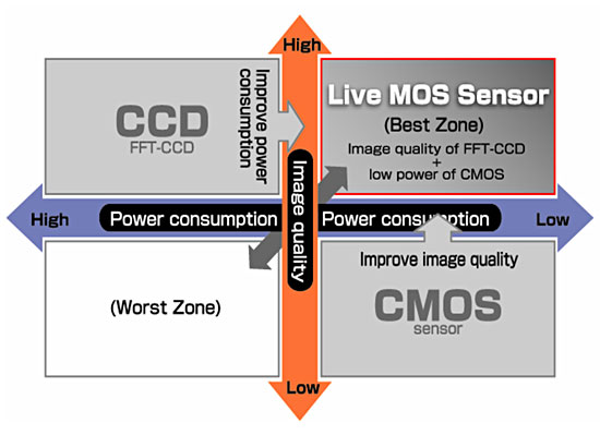
The Live MOS Sensor offers image quality comparable to a Full Frame Transfer (FFT) CCD sensor with the low power requirements of a CMOS sensor, and is noteworthy for its high-quality imaging capabilities over an extended period of time. Simplified circuitry that reduces the distance from each photodiode to its corresponding on-chip microlens assures excellent sensitivity and image quality even when light strikes it at a high angle of incidence.
1. Resolution: 7.5 megapixels, with excellent low-light performance characteristics.
2. Grain: low-noise technologies assure reduced graininess.
3. Tonal range: Simplification of the transfer register and other circuitry results in a large photodiode surface area for FFT-CCD-level sensitivity and responsiveness.
4. Low power consumption: Power requirements are approximately half those of FFT-CCD sensors.
5. High speed: Simple circuit structure contributes to faster processing overall.
Merit of LiveMOS Sensor
Redesigned Sensor Elements with Greater Photosensitive Surface Area
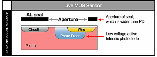
The photosensitive area accounts for around 50% (according to Olympus test method) of sensor element surface (comparable to CCDs). The Live MOS Sensor takes advantage of the simplified circuit requirements and thinner layer structure of NMOS type sensors to offer a larger photosensitive surface area. In addition, circuit technology refinements were made to boost light utilisation efficiency and improve image quality.
A new transfer mechanism for photodiode signal readout enabled us to reduce the number of circuit paths to two, the same as in a CCD sensor, and thereby minimise the surface area that is unresponsive to light. By effectively enlarging the photosensitive surface area and enabling it to capture light that was previously lost, we were able to achieve both high sensitivity and superior image quality. We also developed a new low-noise photodiode signal amplification circuit to further improve sensitivity.
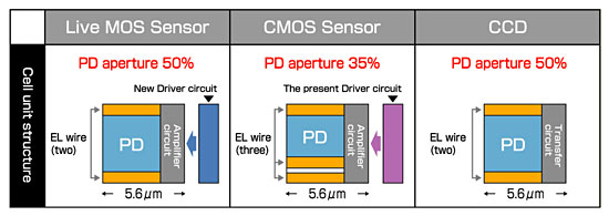
Comparison: Cell unit structure
Low-Noise Technology for Significantly Improved Imaging in Low-Light Environments
A dedicated processing technology developed for use in 5V (design specifications: 2.9V) low-voltage systems is employed to significantly reduce noise. Operating signal noise was also considered, and the sensor photodiodes were deeply embedded in silicon to isolate them from noise-causing elements on the chip surface. As a result, images are clearer, and the graininess and white noise that often appear when shooting in low light are suppressed. Thanks to this technology, low-light performance is improved overall, and a clear image can be obtained even when shooting in very dim light.